If you are looking for Layer Pcb Layout you've come to the right place. We have 30 images about Layer Pcb Layout including images, pictures, photos, wallpapers, and more. In these page, we also have variety of images available. Such as png, jpg, animated gifs, pic art, logo, black and white, transparent, etc.

Not only Layer Pcb Layout, you could also find another pics such as Graphics Card, Circuit Board, Clean Room, Half Wave Rectifier, Chassis Ground, Drafting Table, Linear Voltage Regulator, 16 Pin IC, Signal Generator, High Speed, Bridge Rectifier, Tube Amp, 6 Layer, A4 Size, My85 DTV, 地与电源, Judul Design, SD Card, 1553B, CPC 6128, Panel, PR74, and Đuc Via.


 480×311
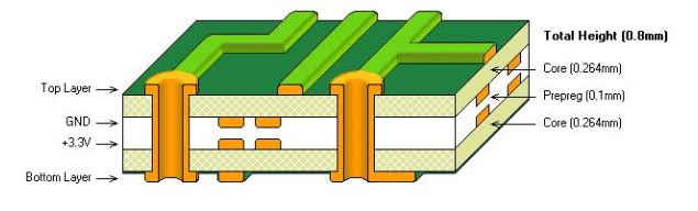
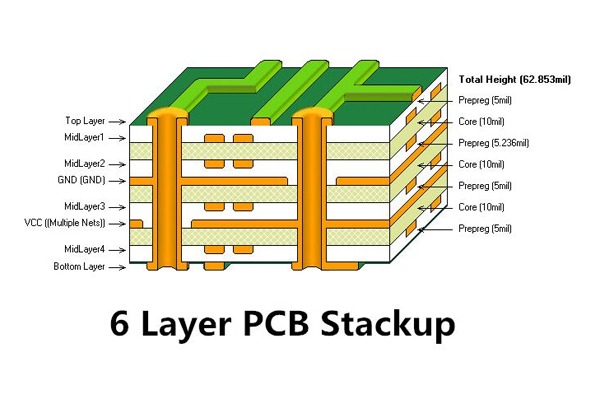
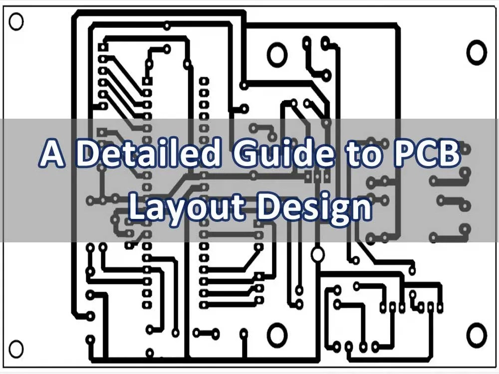
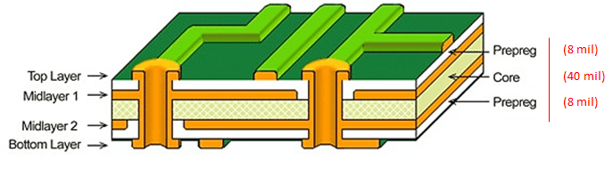
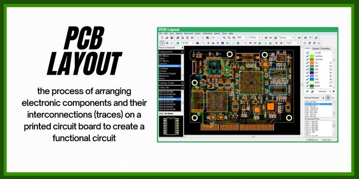
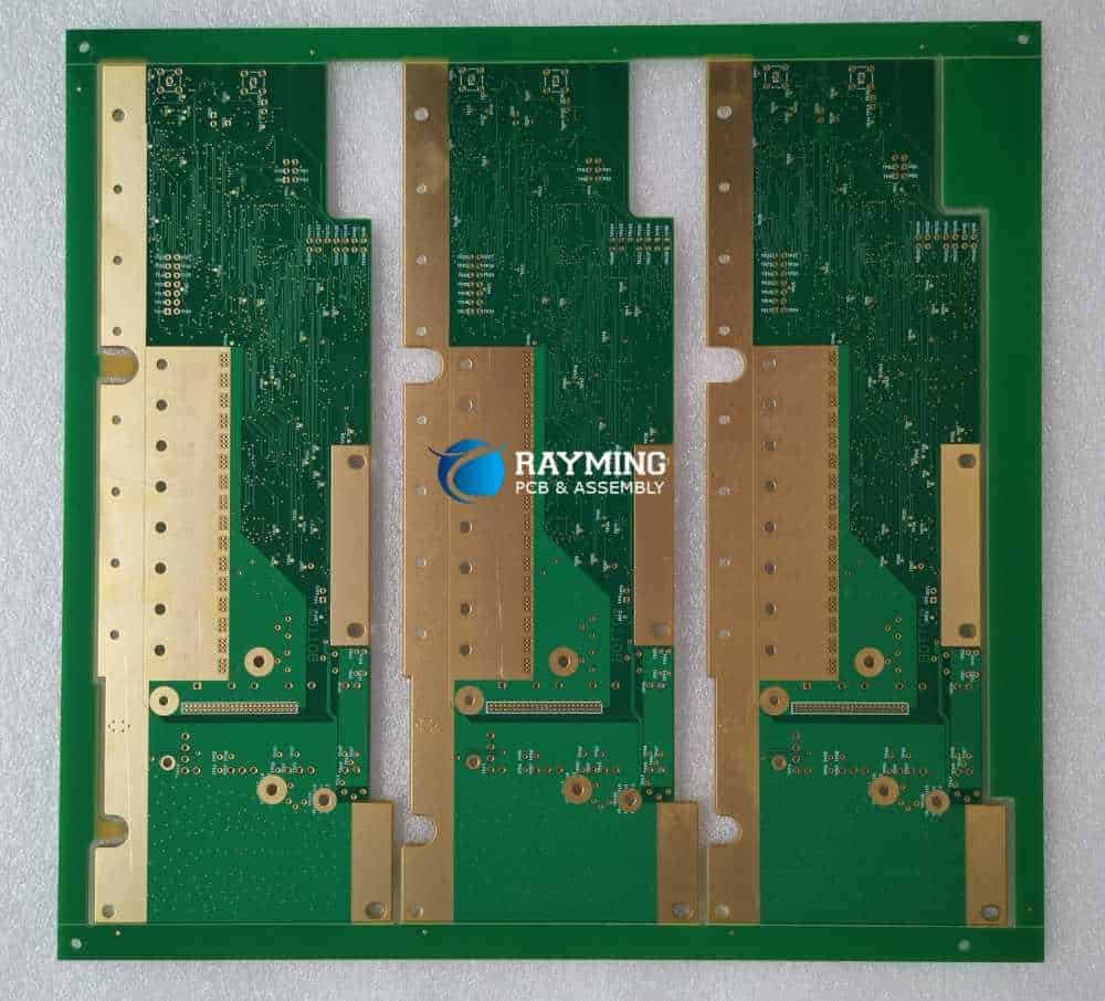
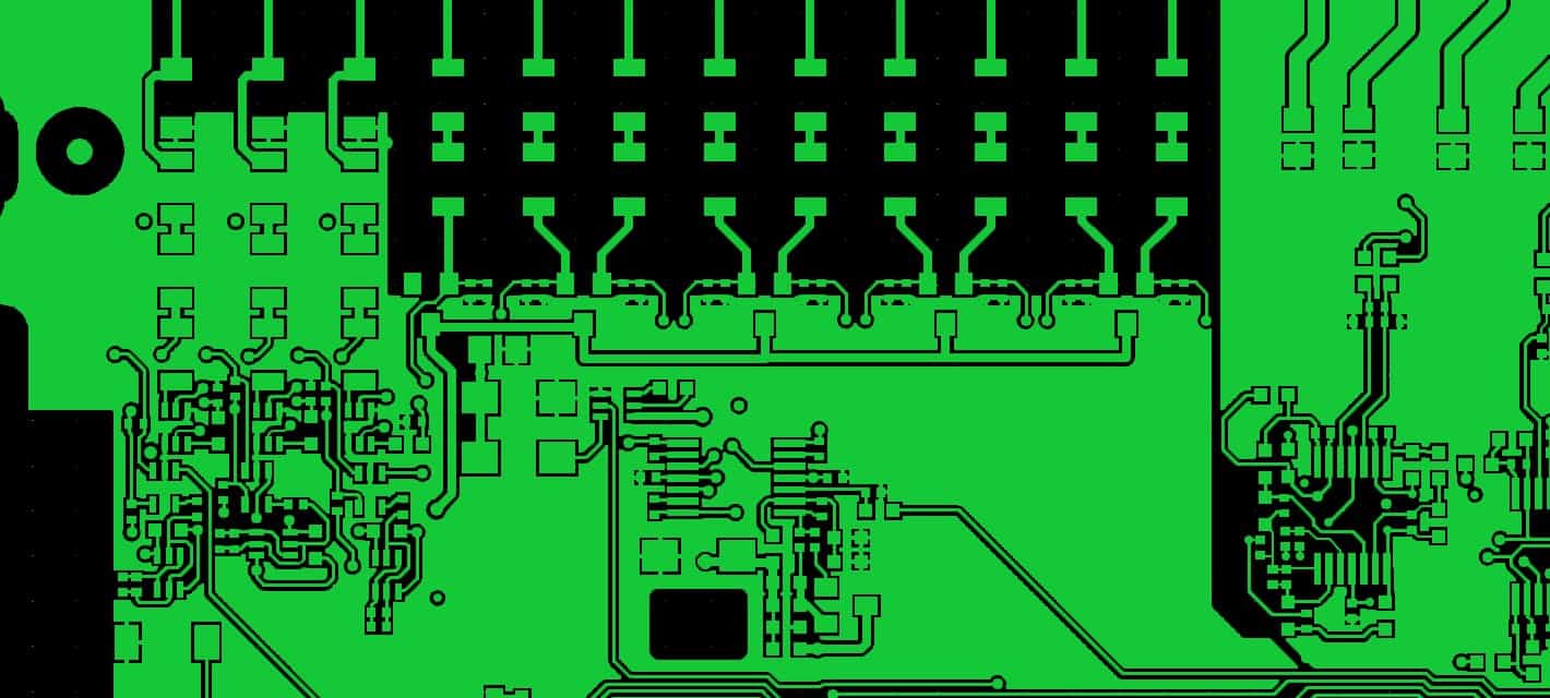
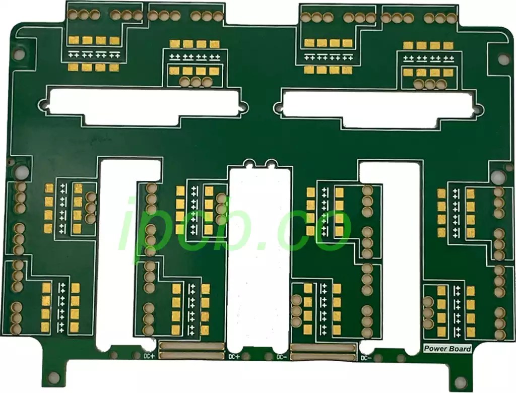
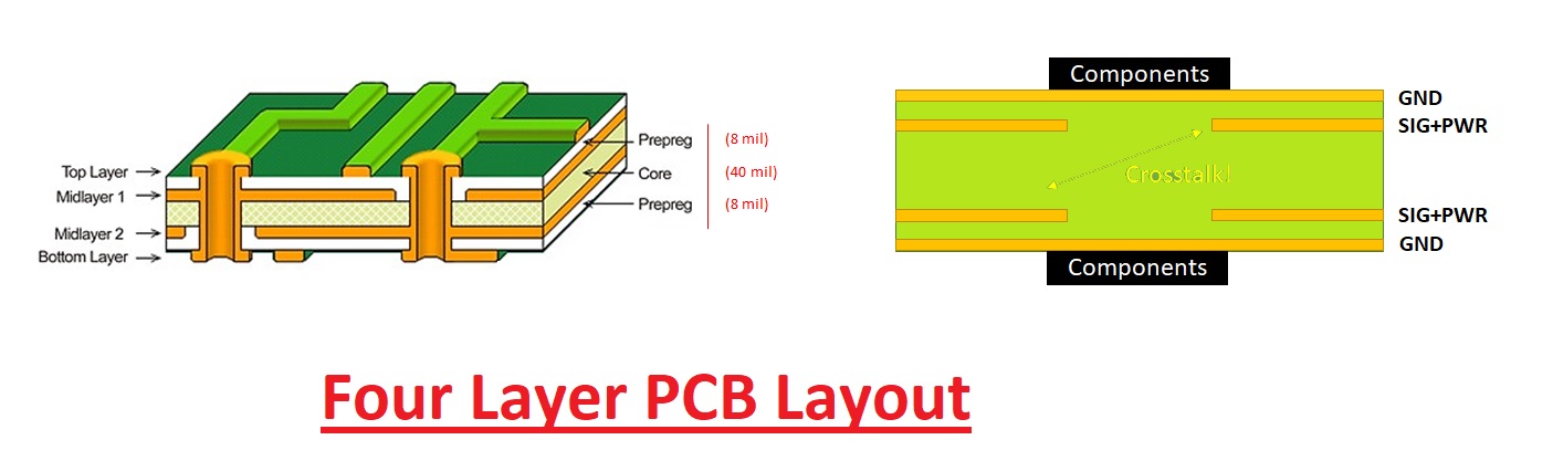
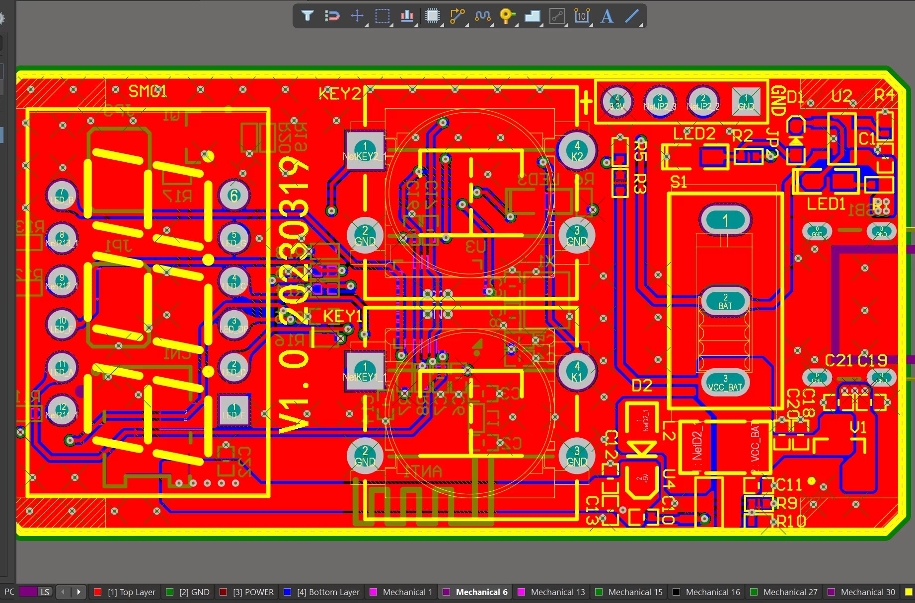
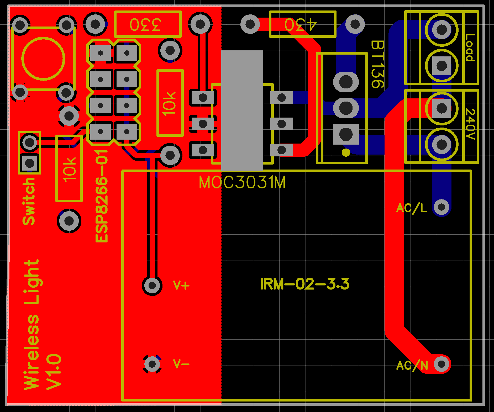
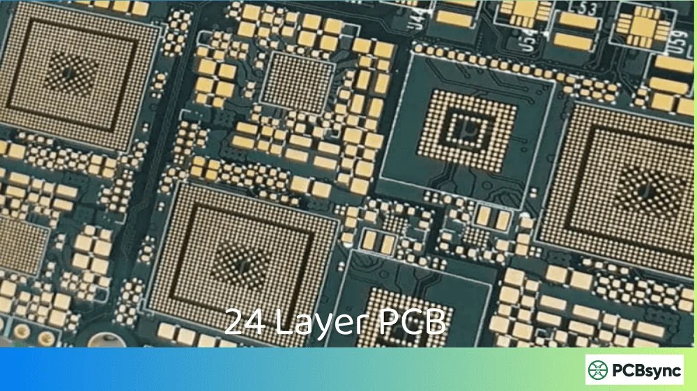
pcb design multi layer pcb layout motherboard pcb layout electronics


Don't forget to bookmark Layer Pcb Layout using Ctrl + D (PC) or Command + D (macos). If you are using mobile phone, you could also use menu drawer from browser. Whether it's Windows, Mac, iOs or Android, you will be able to download the images using download button.